This course is designed to help VLSI career aspirants in the field of VLSI Physical Design. It covers complete details from VLSI design specification till VLSI IC physical design flow, helps to acquire suffiecient skills as needed by Industry. Course modules are designed as per Industry needs and provides complete indepth knowledge to handle challenges in VLSI Back End Flow. Aspiring candidates will learn complete knowledge from netlist to GDS2, by working on advanced lower nanometer technology nodes. The course will benefit VLSI Engineers seeking to enter into VLSI backend design job. In this role engineers will be working for Block & full chip level Physical Design Implementation.
The main focus of the course is to make each engineer understand physical design of IC from netlist through GDSII, creating physical layout representation for each logical functions with in blocks to enable IC fabrication process.
While in course work, for every candidate more emphasis is given on learning through practicals backed by theoritical concepts taught during classes & in the lab sessions.
Eligibility
With Electronics as major subject in B.E/B.Tech/M.E/M.Tech, atleast 60% throughout academic
career. Basic knowledge in Verilog/VHDL, Good knowledge on Digital design, Good knowledge
on any Microcontroller/Processor architectures, and Good logical & analytical ability
Selection based on written test and personal Interviews for eligible interested Candidates.
Syllabus for written test covers Digital logic design, Processor architecture, and Analytical and
Logical questions. Please walkin/mail/call us to schedule for written test & personal interview.
Working VLSI/Software
professionals will get direct admissions.
Course Outline
Overview of Digital design methodology, Representations of Digital Design and
understanding of digital systems, logic gates, combinational and sequential logic. Review
HDL’s and RTL implementation of digital logic systems.
Introduction to semiconductor technologies, logic gates, Review CMOS basics, CMOS
digital design concepts. Understanding CMOS process parameters and characterization of
logic gates
Overview of ASIC/SOC design flow, Digital Design Concepts and Physical Design flow
setup. Review of ASIC fundamentals & fabrication methodologies.
a) Introduction to digital design
b) Number representation, complements and Boolean logic
c) Basic logic gates and logic functions
d) Optimization techniques for logic functions
e) Design of combinational circuits.
f) Implementation and analysis of combinational circuits like, adders, comparator, multiplier etc.
g) Design of synchronous sequential circuits.
h) Implementation and analysis of sequential circuits Flip-Flops, registers, counters, and simple processor
i) Design of Asynchronous Sequential Circuits
j) Design of Finite State Machines (FSM)
k) Discussion - Special circuits like LFSR, FIFO, barrel shifter etc.
l) Case study – PROTOCOLS LIKE AHB, APB, PCI, UART etc.
a) Introduction to Verilog HDL.
b) Gate-Level modeling.
c) Dataflow modeling.
d) Operators.
e) Data types.
f) Modeling timing and delays.
g) Behavioral modeling.
h) Parameters, tasks and functions.
i) Compiler directives.
j) System tasks.
k) File input/output.
l) Switch-level modeling.
m) User Defined Primitives.
n) Design examples – FSM, ALU, RAM, ROM, UART, Traffic light signal.
a) Introduction to ASIC's and ASIC flows
b) Insight into various ASIC design Architecture
c) Writing RTL for ASIC design flow
d) ASIC Design Flow using Synopsys and cadence Tools
e) Using special digital modules in ASIC design
f) Static RAM and Dynamic RAM
g) Clock and Reset managements, power sequencing
h) Clock gating and low power designs
i) Dedicated arithmetic functions
a) Simulation and synthesis issues.
b) RTL design strategies.
c) Static timing analysis.
a) Introduction to STA
b) Comparison with DTA
c) Timing Path and Constraints
d) Different types of clocks
e) Clock domain and Variations
f) Clock Distribution Networks
g) How to fix timing failure
h) Introductions to timing static and dynamic hazards,
i) Path delay, Gate delay, Metastability states.
j) Sequential timing delays like set-up time, hold time,
k) Maximum frequency, violations, slew, slack.
l) Delay analysis
m) Sequential logic pad to set up,
n) pad to pad,
o) clk to next Reg,
p) Reg to o/p and
q) Reg to Reg. violations wrt sequential circuit.
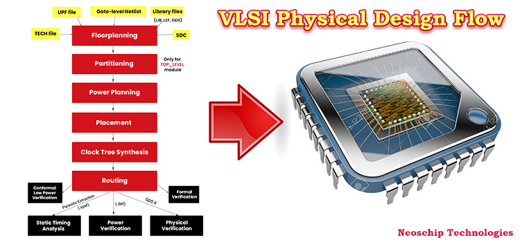
Design data preparation, process technologies and standard cell libraries. Understanding
of standard cell technology parameters, netlist generation and technology mapping.
Reviewing timing constraints and IO constraints. Low power and low area design
concepts
Implementation of RTL design and synthesis, generating netlist and estimating
performance of synthesized design. Area/timing report checks, design constraints for
synthesis. Efficient synthesis techniques. SDF generation
Design plan for hierarchical and flat design implementation, better partition techniques
and flow setup. Special cells and IO cells usage planning, congestion removal techniques and implementation constraint setup.
Understanding various floor planning techniques, setting up guidelines for better floor
planning and meeting design goals. IO PAD placement planning, power planning.
Adding power rings and power mesh.
Placement techniques, various optimization techniques to avoid design congestion.
Performing timing analysis at various levels of floor planning. Pre and post placement
optimization technique, setting up placement goals to meet design placement constraints,
fixing placement issues.
Implementation of clock tree in placed design, understanding various aspects of timing
parameters like clock setup/hold, skew and latency issues, Adding buffers in clock tree
and implementing clock tree. Analyzing timing reports after clock tree synthesis and
fixing issues.
Various types of routing, trial route, special route, global routing and detailed routing.
Analyzing routed design checking post routed design issues, DRC checks, timing checks,
optimization of routing constraints.
Doing complete path and module based timing analysis, checking timing optimizer
reports, identifying failing paths, fixing issues. Extracting capacitor table values for the
design. IR drop and electro migration analysis.
Very happy to get trained in vlsi physical design from neoschip Technology, got oppurtunity to learn from basics to full chip implementation. very good lab facilities with 14+ expirience facuilty.
Excellent training provided in VLSI Physical design, this institute is best in Bangalore for VLSI training. Thanks to Neoschip for helping to get my dreamjob

Sunil K L
Very happy to get trained in vlsi physical design from neoschip Technology, got oppurtunity to learn from basics to full chip implementation. very good lab facilities with 14+ expirience facuilty.